


Date: Jan 30, 2023 Read: 27251
Share:


1. From the Performance Improvement of Flash System
For application scenarios from secure digital (SD) memory card, mobile phone, tablet and other consumer products to enterprise data center, NAND Flash, with such characteristics as high performance, large capacity, low power consumption and low cost, is very popular among users and currently the most widely used semiconductor non-volatile storage medium. In order to meet the increasingly demanding performance requirements of business scenarios, developers have thought of many ways to improve the performance of NAND Flash-based systems, which can be divided into the following categories:
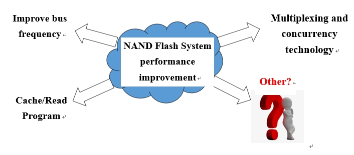
Fig. 1 Overview of Flash System Operformance Improvement
- Improve Bus Frequency and Optimize AC Timing: On the premise of satisfying reliable transmission, upgrade NAND Flash bus frequency and use as few timing parameters as possible for operation. Especially, in the case of the increasing Page Sizes (2KBà4KBà8KBà16KB), it is particularly important to optimize the timing parameters to reduce the time of data transmission via the bus, which has been the direction of continuous efforts over the past 20 years, for example, when the bus interface speed is 200Mbps (100MHz), it takes about 40us to complete 4KB data transmission, but if the bus interface speed is increased to 1600Mbps (800MHz), it only takes about 5us to complete 4KB data transmission.
- Use Cache Read/Program: In general, LUN (Logic Unit Number) is the smallest logical operation unit of NAND Flash, in which read/ write operations are serially executed, i.e., the next read/write operation can be carried out only after a read/write command is completed. Cache Read/Program allows the user to perform read/write data transmission via the bus concurrently when the NAND Flash Array is Busy, thus improving the efficiency of the pipeline.
- Multiplexing and Concurrency Technology includes: 1) Inter-channel concurrency, allowing the user to execute independent commands and data operations concurrently via different channels; 2) Intra-channel concurrency, that is, Interleaving operation, allowing the user to execute interleaving operations between different CEs in the channel or different Dies in the CE under certain constraints; 3) Multiple-plane operation, that is, Multi-Plane operation, allowing the user to concurrently read/write different planes within the Die. It can be said that it is precisely because of the multiplexing and concurrency technology that enables NAND Flash-based solid state storage products achieving GB-level reading & writing performance.
It is obvious that the above optimization covers NAND Flash basic timing/command optimization to the comprehensive optimization of system level, which can be used in combination in the light of the system requirements in practical applications. After years of development, Cache Read/Program and multiplexing and concurrency technology have been developed relatively mature, in contrast, their changes in recent years are relatively small, but NAND Flash bus frequency upgrading technology has been booming, and in recent years there is a trend of accelerated evolution. Below, we will feel the evolution of NAND Flash interface speeds with that of ONFI protocols.
2. The Evolution History of ONFI Interfaces
Founding in May 2006, Open NAND Flash Interface (ONFI) aims to simplify the integration and promotion of NAND Flash in consumer electronics applications and computing platforms. Since the release of the first ONFI protocol in December 2006, ONFI has released dozens of updated versions, and the maximum interface speed has also been developed from the initial 50Mbps to the latest 3600Mbps. Fig. 2 shows the evolution trend of interface speeds continuously optimized in line with ONFI protocols.
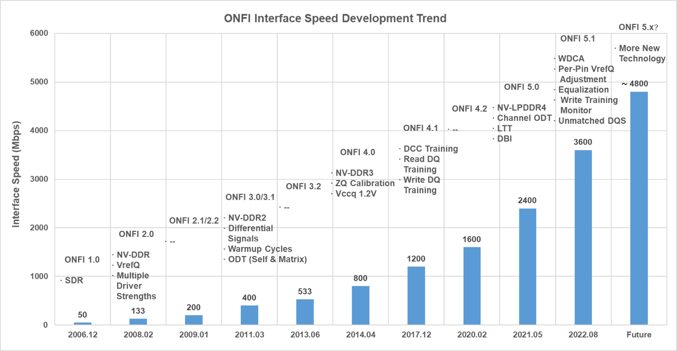
Fig. 2 Evolution of ONFI Interface Speeds
- ONFI 1.0: With the successful application of NAND Flash in consumer electronic products such as SD memory card and IPod, as well as the increasing demand for NAND Flash-based MP3 and U disk, the application field of NAND Flash has been greatly expanded. However, due to the different interface protocols of different NAND Flash manufacturers, the downstream master chip manufacturers and product manufacturers encounter various compatibility problems. In order to change this situation, Intel led the establishment of ONFI, and soon after launched ONFI 1.0, aiming to unify NAND Flash interface protocols.
- ONFI 2.x: ONFI 2.x introduced NV-DDR technology to achieve Double Data Rate through double-edge sampling, with maximum interface speed evolved from 133Mbps of ONFI 2.0 to 200Mbps of ONFI 2.1/2.2. NV-DDR technology introduced an external reference voltage as the sampling reference of data I/O signals, and used a source synchronous clock to accurately latch data, commands, and address signals. However, because DQS and Clock are not differential signals, the edge is prone to interference. Currently, NV-DDR interfaces are rarely seen in mainstream consumer/enterprise NAND Flashes.
- ONFI 3.x: ONFI 3.x introduced NV-DDR2 technology, with maximum interface speed evolved from 400Mbps of ONFI 3.0/3.1 to 533Mbps of ONFI 3.2. NV-DDR2 introduced Differential Signal and On-Die Termination (ODT) technology to improve the signal quality. In the differential mode, noise and interference can be effectively suppressed by enabling the RE_n/RE_c differential signal pairs and DQS_t/DQS_c signals differential signal pairs during the stage of data transmission. By integrating the ODT terminating resistor on the NAND Flash chip, the impedance mismatch between the controller and the signal transmission channel of NAND Flash can be minimized, which helps to reduce the signal reflection. In addition, the ODT resistance value can be controlled from software configuration register, thus greatly simplifying the hardware circuit design.
- ONFI 4.x: ONFI 4.x introduced NV-DDR3 technology, with maximum interface speed evolved from 800Mbps of ONFI 4.0 to 1600Mbps of ONFI 4.2. In order to ensure the quality of high-speed signal transmission, NV-DDR3 introduced several calibration techniques, including ZQ Calibration, Duty Cycle Correction (DCC) and read/write DQ Calibration. As mentioned above, ONFI 3.0 introduced ODT technology. Due to the ODT resistor on NAND Flash is prepared by CMOS process, resistance value is prone to drift when the temperature and voltage change, so it is necessary to calibrate the resistance value by external high-precision resistor through ZQ Calibration technology. DCC Calibration allows adjusting the signal duty cycle to solve the mismatch between rising edge and falling edge caused by the asymmetry of high-speed signal transmission path, while read/write DQ Calibration ensures that read/write sampling signal is aligned to the center of eye diagram.
- ONFI 5.x: ONFI 5.x introduced NV-LPDDR4 technology, with maximum interface speed evolved from 2400Mbps of ONFI 5.0 to 3600Mbps of ONFI 5.1. To address the tremendous challenge of signal integrity posed by the high-speed interface, ONFI 5.x introduced an asymmetric DQS design and an adaptive equalizer design in addition to further strengthening read/write DQ Calibration and VrefQ Calibration. For example, DFE (Decision Feedback Equalizer) technology uses the output of the last channel to be weighted and fed back to the input after judgment, so as to eliminate the post-symbol interference. In addition, NV-DDR3 and NV-LPDDR4 support the same maximum interface speed, but the advantage of NV-LPDDR4 is that the power consumption of read operation can be greatly reduced after using LTT technology.
From ONFI 1.0 to the recently released ONFI 5.1, it can be seen that in order to match the increasingly demanding bandwidth requirements of the system front interfaces (e.g. eMMC/UFS/PCIe), NAND Flash interface speed has been increased by 72x, and will quickly be moved to the next peak in the future.
Then, is the increase in interface speed doubling the benefit of the system? The answer is NO.
3. The Inadequate Traditional Protocols Call for Further Improvement
The signals transmitted via the NAND Flash bus can be divided into three types: Commands, Addresses, and Data. Through DQ[7:0] time division multiplexing, commands, addresses and data are respectively transmitted at different times. Among them, the data is synchronous transmitted and differentially sampled, the rate is high. However, commands and addresses are asynchronously transmitted and single-ended sampled, and the rate is low. From ONFI 1.0 to ONFI 5.1, the interface sppeeds have been developed rapidly, but the transmission form of commands, addresses and data is basically the same. In fact, with the increase of bus transmission speed, the main improvement is the data transmission delay, and the transmission delay of commands and addresses has not been improved, thus, for the system, the bus use efficiency is decreasing. Fig. 3 below is a comparison of bus efficiencies under optimistic write/read scenarios. Obviously, the bus efficiencies under both read and write scenarios gradually decrease, especially when the bus efficiency under read scenario drops to about 50%, which further aggravates the challenge of system design.
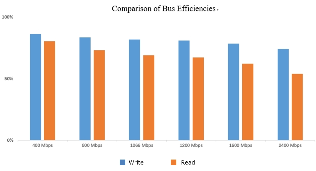
Fig. 3 Analysis on NAND Flash Bus Efficinecies
Taking a certain model of SSD in the industry as reference, Fig. 4 shows the comparative analysis of it with UH811a, an ESSD developed by Union Memory. It can be seen that the read bandwidths of the two SSDs are equivalent, about 7000MB/s, but the 4K random read IOPS of UH811a is significantly improved compared with the reference SSD. It’s found from further analysis that the 4K IOPS of UH811a after conversion is equivalent to the read bandwidth. However, after the same conversion, the bandwidth of the reference SSD is only 70% of the read bandwidth, the reason is that the expenditure of bus random read operations is higher than that of sequential read ones.
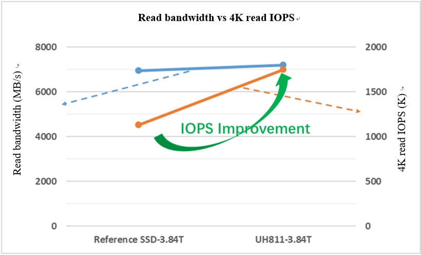
Fig. 4 Read Bandwidth vs 4K Read IOPS
It can be seen that in the case of unchanged transmission form of the traditional commands/addresses/data, with the improvement of interface speed and the increase of system complexity, the resultant benefits are attenuated. Therefore, the deficiencies of the traditional protocols facilitate the continuous improvement of the protocols. In the face of this problem, Joint Electron Device Engineering Council (JEDEC) is intensively discussing the next round of evolution of protocols, and the interface speed will be improved while optimizing the command/address transmission mode, which is bound to create a new test to the design of master chips.
4. Conclusion
Traditionally, improving NAND Flash interface speed is the main means to improve system performance, and NAND Flash manufacturers have come up with various ways to solve the problem of signal integrity caused by high-speed signals. Facing the future, the traditional input mode of commands/addresses leads to low bus utilization, the further evolution of protocols will also usher in new input mode of commands/addresses in addition to the consideration of continuously improving the interface speed. Union Memory will pay close attention to the development trend of protocols and compatibly support the future media with a flexible architecture, so as to bring better storage products and solutions to the customers.
References
1. ONFI spec, http://www.onfi.org/specifications
2. 2022, Phison, NAND Flash 101: Flash Device Interfaces,https://phisonblog.com/nand-flash-101-flash-device-interfaces-2/
3. 2021, Evolution of Mobile NAND Flash-based Storage, https://phisonblog.com/the-evolution-of-mobile-nand-flash-memory-storage-2/
4. Mathematics in the Chips ——Equalizer (EQ) and Its Applications in External High-Speed Bus, https://zhuanlan.zhihu.com/p/48343011

Address: 19th Floor, Block B, Ramaxel Houhai Center, Nanshan District, Shenzhen
Tel: +86 755-2681 3300
E-mail: support@unionmem.com
